The chip that controls the display on your phone, laptop, car dashboard or television may soon have a Noida region connection.
A major semiconductor unit is being set up near Jewar airport in the Yamuna Expressway Industrial Development Authority area. The project is being developed by India Chip Pvt. Ltd., a joint venture between HCL Group and Foxconn Hon Hai Technology India, and has been approved under the Government of India’s India Semiconductor Mission.
This is not just another industrial plot allotment in the Yamuna Expressway belt. It marks a shift in the region’s growth story.
For years, the YEIDA belt has been discussed mainly through the lens of real estate, warehousing and the upcoming Noida International Airport. The HCL-Foxconn semiconductor unit adds a new layer: high-value electronics manufacturing, skilled jobs, supply-chain development and a potential technology corridor anchored around Jewar.
The Press Information Bureau describes the facility as an Outsourced Semiconductor Assembly and Test, or OSAT, unit to be set up at YEIDA by India Chip Pvt. Ltd. under the Modified Scheme for Semiconductor Assembly, Testing, Marking and Packaging, with an investment of over ₹3,700 crore.
What Exactly Is Being Built?
The project is officially the HCL-Foxconn Joint Venture project, India Chip Pvt. Ltd.
This is not a full semiconductor fabrication plant. Instead, it is an OSAT facility.
OSAT stands for Outsourced Semiconductor Assembly and Test. Such a unit handles the later stages of semiconductor manufacturing. It receives processed wafers, assembles and packages individual chips, tests them to verified specifications, and prepares them for integration into finished electronic products.
That may sound like a secondary step, but it is a critical one. Without assembly, testing and packaging, processed wafers cannot become usable components. There is no phone screen, laptop display or car dashboard without this stage of the chain.
According to PIB, the YEIDA facility will support sectors including mobile phones, tablets, laptops, automobiles and consumer electronics. The same official release says the project will help build domestic manufacturing capacity, reduce import dependence and strengthen supply-chain resilience.
HCL Group’s own official release describes the project as the HCL Group and Foxconn joint venture OSAT facility in YEIDA, Greater Noida, with the foundation stone laid on February 21, 2026.
Where Is the Project Coming Up?
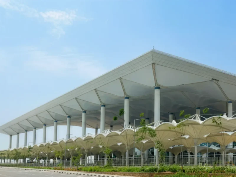
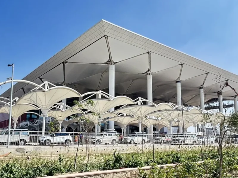
The unit is being set up in the Yamuna Expressway Industrial Development Authority area, near the upcoming Noida International Airport at Jewar.
PIB’s May 2025 Cabinet approval note confirmed that the plant, approved under the India Semiconductor Mission, would be set up near Jewar airport within YEIDA.
For residents of Noida, Greater Noida and the Yamuna Expressway belt, the location matters because it sits at the intersection of three major growth drivers:
- The Noida International Airport at Jewar
- The Yamuna Expressway industrial corridor
- The wider Noida-Greater Noida electronics and technology ecosystem
This is why the project should not be read in isolation. It is part of a deliberate effort to build an advanced manufacturing zone around the airport, not simply fill industrial plots.
What Will the Unit Make?
The plant will manufacture display driver chips, formally known as Display Driver Integrated Circuits, or DDICs.
These are the chips that translate data from a device’s processor into the electrical signals that light up each pixel on a screen. Every phone, laptop, PC, car dashboard, television and consumer device with a display needs one.
PIB’s Cabinet approval note confirms the production targets:
- 20,000 wafers per month
- 36 million units per month
The unit is designed to serve demand from mobile phone, laptop, automobile, PC and consumer electronics manufacturers. It directly addresses a segment of the semiconductor supply chain where India has had limited domestic production capacity.
Why OSAT Matters for India
India has strong software talent and a large, growing electronics market. What it has been building, through programmes such as the India Semiconductor Mission, is a foothold in semiconductor manufacturing itself.
A semiconductor supply chain has several distinct layers: chip design, wafer fabrication, assembly, testing, packaging, materials, equipment and logistics. OSAT belongs to the assembly, testing and packaging layer. That entry point is both practical and strategic.
OSAT facilities require genuine technical capability: cleanroom environments, precision machinery, process engineering, quality control and trained workforces. They also create real demand for skilled employment across multiple disciplines:
- Semiconductor process engineers
- Precision assembly and packaging technicians
- Quality and reliability engineers
- Test equipment operators
- Cleanroom maintenance specialists
- Supply-chain and logistics professionals
PIB has noted that the project is expected to foster innovation, skill development and technology transfer, while creating thousands of direct and indirect employment opportunities for engineers, technicians and professionals.
Why Jewar Airport Gives the Project a Strategic Advantage
Semiconductor chips are high-value, low-weight cargo. They move on tight supply-chain schedules. Air freight is a major logistics route for high-value electronics and semiconductor components.
A manufacturing facility located near an international airport with planned cargo infrastructure has a structural cost and speed advantage over a facility that must route goods over long road distances before reaching air freight connectivity.
That is why the YEIDA location is strategic.
The airport is not incidental geography. It is part of the larger industrial planning around the Yamuna Expressway region. If cargo infrastructure, road connectivity and industrial services develop as planned, the area could become more attractive for suppliers, service providers and ancillary electronics manufacturers.
PIB also notes that global semiconductor supply-chain partners are already preparing for India’s semiconductor growth. Applied Materials and Lam Research have established an India presence. Merck, Linde, Air Liquide, Inox and other gas and chemical suppliers are also gearing up for growth in India’s semiconductor industry.
What It Means for Noida and Greater Noida
For the Noida region, the project matters for three reasons.
First, it upgrades the region’s industrial identity. The Noida-Greater Noida belt is already home to IT services, mobile manufacturing, electronics assembly, media production and education. A semiconductor OSAT unit adds a higher-complexity manufacturing layer to that mix.
Second, it connects the airport story to a real industrial use case. The Noida International Airport is not only about passenger flights. Semiconductor exports, precision cargo logistics and high-value manufacturing are among the economic activities that airport-adjacent industrial zones are designed to support.
Third, it creates a new skills conversation for local institutions. Semiconductor-related work requires trained engineers and technicians. Greater Noida has a strong concentration of engineering and technical institutions. If local colleges align courses, internships and practical training with the requirements of the semiconductor sector, students and graduates from Noida, Greater Noida, Jewar, Bulandshahr and nearby districts could benefit.
On employment, PIB says thousands of direct and indirect jobs are expected once the facility is operational. State-level approval documents, as reported by Times of India in October 2025, cited a figure of 3,780 direct and indirect jobs. These are projections tied to full commissioning, not immediate hiring. The employment impact will develop over the coming years.
Why the Project Is Being Watched Closely
Semiconductor projects are infrastructure-intensive. They need reliable power, water systems, road connectivity, precision-grade civil construction, cleanroom environments, safety arrangements and consistent policy support. Progress on each of these determines the execution timeline.
The foundation stone ceremony took place on February 21, 2026. Prime Minister Narendra Modi participated virtually, while Chief Minister Yogi Adityanath and Union Minister for Information Technology Ashwini Vaishnaw were present at the YEIDA site.
The UP government has also put a detailed incentive package in place, as approved by the UP Cabinet in October 2025. Reported support includes capital subsidy under UP Semiconductor Policy-2024, land-related relief, stamp duty exemption, electricity duty waiver and housing support for employees near the plant.
The project is expected to be operational around 2028, subject to construction and commissioning timelines.
The Bigger Picture: Noida-YEIDA as a Technology Corridor
This project fits into a larger industrial shift across the Noida-Greater Noida-YEIDA belt.
The region is no longer being shaped only by residential townships, office towers and retail development. Several higher-value growth themes are now active simultaneously:
- Noida International Airport
- Data centres in Noida and Greater Noida
- Electronics manufacturing clusters
- Global capability centres of multinational companies
- Semiconductor and component manufacturing
- Medical device manufacturing
- Logistics and precision warehousing
The Government of India also approved a ₹417 crore Electronics Manufacturing Cluster under the EMC 2.0 scheme in Gautam Buddha Nagar in June 2025. According to PIB, the cluster will be developed by YEIDA, spread over 200 acres, and is expected to attract ₹2,500 crore in investment while generating 15,000 jobs.
PIB says the cluster will support manufacturing across consumer electronics, automotive and industrial electronics, medical devices, computer hardware and communication equipment. It is also expected to provide plug-and-play infrastructure, shared facilities, standard factory sheds, electricity, water, sewage treatment, hostels, skill development centres and health centres.
That makes the HCL-Foxconn semiconductor unit part of a wider industrial picture. It is not the only project in the corridor, but it is one of the most significant anchor investments in the region’s emerging electronics and semiconductor story.
What Residents Should Watch Next
For residents, job seekers, students and businesses in the Noida region, these are the milestones that will signal how the project is progressing:
- Civil construction updates at the YEIDA site
- Power grid and water infrastructure readiness
- Cleanroom construction and machinery installation announcements
- Hiring or internship launches from India Chip Pvt. Ltd.
- Skill development partnerships with local engineering colleges
- Cargo terminal progress at Noida International Airport
- New supplier or ancillary investment announcements in YEIDA’s electronics cluster
- Progress on the EMC 2.0 electronics cluster in Gautam Buddha Nagar
The real impact of this project will not be measured by the foundation stone or investment figure. It will be measured by jobs created, suppliers developed, institutions aligned and whether young people from this region can build careers in a sector the country is now treating as a strategic priority.
Why This Story Matters for Pulse of Noida Readers
The phone screen in your hand, the laptop on your desk, the display in your car: all of these depend on semiconductor supply chains. One part of that chain is now being built near Jewar airport, close to the Noida-Greater Noida region.
The HCL-Foxconn semiconductor unit at YEIDA will not transform the region overnight. But it is a serious, officially approved, foundation-stone-laid project backed by both central and state government commitments.
If executed well, it could become one of the anchor projects that changes how the Yamuna Expressway belt is understood: not only as land near an airport, but as a future technology and manufacturing corridor.
Have a Noida business, infrastructure or city progress story to share?
Pulse of Noida is building a deeper record of the people, projects and institutions shaping Noida, Greater Noida and the Yamuna Expressway region. If you know about a verified development, local initiative, business expansion, civic issue or community story, share the details with us.
Official Sources and References
- Press Information Bureau, February 20, 2026: PM to participate in groundbreaking ceremony of HCL-Foxconn Joint Venture project, India Chip Pvt. Ltd. Read source
- Press Information Bureau, May 14, 2025: Cabinet approves semiconductor unit in Uttar Pradesh under India Semiconductor Mission. Read source
- HCL Group, February 21, 2026: Foundation stone for India Chip Pvt. Ltd. in Jewar. Read source
- Press Information Bureau, June 25, 2025: ₹417 crore Electronics Manufacturing Cluster approved in Gautam Buddha Nagar, Uttar Pradesh. Read source
- Times of India, October 8, 2025: UP Cabinet incentive package and employment projection for the HCL-Foxconn unit. Read source
Editorial note: Some media reports have referred to the investment figure for this project as ₹4,000 crore. Pulse of Noida uses the official PIB figure of over ₹3,700 crore throughout this story.